The page you are viewing is a mirror of the original page constructed by Clint Turner, though not an exact copy (a couple of links have been added).
This is done to help preserve the page's content. View the original page here.
Abstract: This article discusses the design of a simple Class-E switching-type LowFER transmitter.
[Reproduced from Western Update #59, September 1988]
My LowFER beacon, MPM, has been on the air for some time, utilizing a dual MOSFET push-pull transmitter design. Despite it's complexity I've been quite proud of the circuit, which I considered to be hard to beat for DC to RF efficiency. Because I have received several requests for a description of the circuit, and since efficiency has recently become a "hot" topic, I had planned on writing a short article on the transmitter.
However, no sooner had I began than I ran across Frank Cathell's article (WU #58) on Mike Mideke's "simple beacon". I'd previously glanced over Mike's circuit without being particularly impressed: "Maybe 50% efficiency on a good day" I thought to myself. But Frank's article started me thinking that maybe the efficiency could be pretty good if the active device could be operated as a switch. I decided to do a rigorous analysis of the circuit, optimizing component values, and then check the results with a circuit analysis computer program. The results were encouraging, so I went ahead and built a prototype and WOW! - was I ever impressed!!! Not only is it considerably simpler than my push-pull design, the efficiency is higher! As a result, I no longer recommend my push-pull design! However, my analysis uncovered a few surprising characteristics (as well as some minor errors in Frank's article) so, since I still have this ego-driven desire to write something, I thought I'd share my findings with everyone:
As Frank's article pointed out, operating the device as a switch can theoretically achieve 100% efficiency. What originally frightened me about this circuit was that the switch was directly in parallel with the tank circuit. Any voltage on the capacitor when the switch is turned on would be discharged by the switch, dissipating the capacitor energy and wasting power. Since the MOSFET drain voltage oscillates about the supply voltage (rather than ground) when the switch opens, it would not normally return to zero volts after one-half cycle. To remedy this situation, the tank circuit should be DETUNED so that it oscillates for more than one-half cycle while the switch is opened. It turns out that if the tank is made resonant at 1.2915 times the operating frequency (assuming a 50% switch duty cycle) the voltage on the drain will return to very nearly zero volts when the MOSFET turns on. (Contrary to Frank's article, a 50% duty cycle is not necessary - any duty cycle may be used, the only difference being that the detuning factor will change. However, since 50% is easily produced, it is used throughout this analysis.)
It is also desirable for high efficiency that the current in the MOSFET
be zero immediately following turn-on: This tends to minimize average
MOSFET current for a given power output. This will occur if the inductor
is completely discharged during the MOSFET "off" period, i.e., all energy
stored in the inductor is transferred to the load.
|
For a given supply voltage, frequency, and power output, it turns out
that there is an ideal inductance value and load resistance which satisfies
the above condition. When these values are combined with the condition
for tank resonance above, we obtain component values and and load resistance
for our "optimized" circuit:
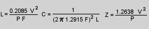
| Where: | |
| L = tank inductance (Henries) | Z = load resistance (Ohms) |
| C = tank capacitance (Farads) | P = output (or input) power (Watts) |
| V = supply voltage | F = operating frequency (Hertz) |
| Also: | |
| Vmax = peak voltage on MOSFET = 3.6311 * V | |
| Irms = rms MOSFET current = 1.1638 P / V |
The above equations are the result of several hours of slaving over a table of Laplace Transforms, and numerical equation solving using a programmable calculator. Since I easily could have made an error in the calculations I decided to check my results using a circuit analysis computer program I have access to at work. I first calculated component values using the above equations, for P = 1 watt, V = 12 volts, and F = 179,000 Hz. These values worked out to:
L = 167.7 uH
C = 2826 pF
Z = 182 ohms
| For reference, the values for L, C, and Z referred to in the past articles
(i.e. "Simple Beacon" schematic) are as follows:
L = 75 uH C = 0.015 uF and Z = 72 ohms |
Note that the values for L and C differ markedly from those given in the "simple beacon" schematic. The value for Z is considerably greater than that given in Frank's article, as well as greater than most LowFER antennas. But since I was now in the magical world of software I could have any antenna impedance I wanted. I modeled the antenna as a 182 ohm resistor, 1000 ohm inductive reactance, and 1000 ohm capacitive reactance all in series. The active device was modeled as a switch in series with a 1 ohm resistor, opening and closing with a 50% duty cycle at a 179 kHz rate.
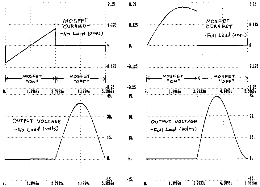
The analysis was run and the output voltage and switch current were
plotted. Plots were made for both no load and full load.
The output voltage closely approximates a half cycle sinewave at no load,
but departs somewhat from sinusoidal at full load. The full load
MOSFET current is seen to be zero when the switch first closes, as desired.
Note also that the no- load MOSFET current is initially negative and ramps
positive, with the result that the average current is essentially zero,
which would be expected for no load.
 |
Encouraged by these results, I decided to build a real working output stage. I picked up an IRF-511 MOSFET at Radio Shack, dug through my junk box and found a T-150-2 powdered iron toroid core, and borrowed several mica capacitors from work which totaled about 2800 pF. I added turns to the toroid until it resonated with the caps at 231 kHz (1.2915 times 179 kHz) - this required 105 turns of #30 wire. I drove the gate of the MOSFET with a 5 volt 50% duty cycle square wave from a function generator. For a dummy load, I used a 150 ohm resistor in series with a 3 mH inductor and 300 pF variable capacitor - the resistance of this combination was very nearly 182 ohms at resonance.
I first powered up the circuit with no load, and observed a output waveform
identical with the no load output voltage plot. The supply current
was about 1.2 mA. I then connected the load, and by tuning the variable
cap obtained a waveform identical to the full load plot, with a supply
current of 83 mA. Using the 'scope I then measured the load current,
and calculated the output power and efficiency, which was an amazing 98%!
The highest efficiency I ever measured with my push-pull design was 95%.
The circuit was well behaved with changes in tuning, with maximum RF output
and maximum current drain occurring very nearly together.
 |
A tune-up procedure which works well is as follows: With no load, the tank is adjusted for minimum supply current (this adjustment is not too critical and the circuit will work well over a +/- 10 kHz range using fixed values). The antenna is then connected and the loading coil tuned for maximum RF. Since most LowFER antennas have a resistance of less than 182 ohms some means of impedance transformation is required. Probably the simplest way of doing this is to connect the antenna and loading coil to a tap on the tank inductor. The position of the tap should be adjusted so the transmitter draws 1 watt DC (83 ma for a 12 volt supply) when the loading coil is tuned for max. RF output. If too much current is drawn, tap the inductor farther from the MOSFET end.
As is obvious from the output voltage plot, the circuit generates considerable
harmonics. A fourier analysis was run using the circuit analysis
program and the amplitudes of the first 10 harmonics were calculated (at
full load):
| Fundamental: 0 dB | 6th -30.24 dB |
| 2nd -5.54 dB | 7th -33.19 dB |
| 3rd -16.92 dB | 9th -35.20 dB |
| 4th -22.66 dB | 9th -37.62 dB |
| 5th -27.06 dB | 10th -38.93 dB |
These numbers may look scary, especially the 2nd, but shouldn't be much cause for alarm. A LowFER antenna with a Q of 100 (a rather mediocre value) will provide 37.5 dB attenuation of the second harmonic, so the radiated second harmonic will be over 43 dB below the fundamental.
For proper circuit operation, the load impedance at all harmonic frequencies should be high compared to the impedance at the fundamental. This is easily accomplished by placing a series tuned circuit in series with the load. A LowFER antenna / loading coil combination provide this automatically, but if the transmitter is going to be driving a transmission line, lowpass filter, pi-network, dummy load, or a tap on a grounded loading coil, a series tuned circuit designed for an operating Q of 5 or greater should be connected in series with the load, and tuned for maximum RF. If a low distortion sinewave is desired (e.g., for efficiency measurements), the Q can be selected based on the above harmonic levels to provide the desired harmonic distortion.
Finally, as Frank's article mentioned, it is important to ensure that the MOSFET gate be driven with a fast risetime squarewave to provide switching-mode operation. Since MOSFETs have considerable input capacitance, a low impedance driving source is needed. I have had excellent results driving MOSFETs directly from HC series CMOS. The HC parts have a driving source resistance of 30 ohms or less, as compared to several k ohms for the 4000 series. I also recommend AC coupling the drive to protect the MOSFET (what if the oscillator stops and the divider output is stuck high??)
In summary, I'm just about convinced that the 'simple beacon" circuit is the Ultimate Design! With the changes outlined here, it provides unmatched DC to RF efficiency, as well as being just about the simplest circuit one could hope for. What could be better?
References:
Go to
the "CT" MedFer PSK Beacon page
This page converted to HTML by Clint, KA7OEI on 20000520.
Updated on 20010727
The page you are viewing is a mirror of the original page constructed by Clint Turner, though not an exact copy (a couple of links have been added).
This is done to help preserve the page's content. View the original page here.