for
|
This page has etching masks which can be used to make printed circuit boards for the Laser Pointer Audio Modulator and Laser Beam Detector/Demodulator. The format is "bigfoot", a large 3" x 6" (8cm x 16cm), single-sided, standard DIP, no-holes (no drilling required), surface mount footprint - easy to make at home. Mirror images are included in case your fabrication process requires that format. Also shown are the parts placement masks (silkscreens). Gerber files for automated commercial board fabrication are also available. Links to the mask files are shown below. Your browser will almost certainly NOT print these files correctly. You'll need an image viewer/manipulator to print these files. If you have Photoshop, you're home free. If not, Irfanview is a versatile image viewer and manipulator that comes absolutely free and highly recommended. Get Irfanview here. Instructions for saving and printing the files begin below the image links. Audio ModulatorDetector/DemodulatorCombinedModulator and Detector/Demodulator masks in a single image. Instructions for Saving the Image Files
Instructions for Printing - Photoshop
Instructions for Printing - Irfanview
Instructions for Saving and Renaming the Gerber Files(Note: A Gerber file is a text file. The file must be renamed as filetype GRB after saving.)
|
| Component Designator |
Number of same value |
Value | |
| C1,C2,C3,C10,C12 |
5 |
.1uF (ceramic) | |
| C4,C7 |
2 |
4.7uF (25v electrolytic) | |
| C5 |
1 |
270pF (mica or metallized film) | |
| C6,C9 |
2 |
1uF (35v tantalum) | |
| C8 |
1 |
.001uF (metallized film) | |
| C11 |
1 |
.01uF (metallized film) | |
| C13 |
1 |
10uF (25v electrolytic) | |
| C14 |
1 |
100uF (16v electrolytic) | |
| D1,D2 |
2 |
1N5817 (Schottky rectifier) | |
| D3 |
1 |
Laser diode (Cheap laser pointer) | |
| D4 |
1 |
1N914 | |
| R1,R2,R8,R10,R14 |
5 |
10k (all resistors 5% 1/4 watt) | |
| R6 |
1 |
2.7M | |
| R3,R9 |
2 |
270k | |
| R4,R5,R7,R13 |
4 |
100k | |
| R11,R12,R15,R16 |
0 |
not used | |
| R17 |
1 |
2.2k | |
| R18 |
1 |
33k | |
| R19 |
1 |
560 Ohm | |
| R20 |
1 |
240 Ohm | |
| R21 |
1 |
2 Ohm | |
| U1 |
1 |
LF347 (Quad JFET opamp) | |
| U2 |
1 |
CD4069 (Hex CMOS inverter) | |
| U3 |
1 |
CD4013 (Dual CMOS D flip-flop) | |
| U4 |
1 |
TC1411 (HS driver)(Digikey TC1411CPA-nd) | |
| U5 |
1 |
LM317 (Voltage regulator) | |
| VR1 (Frequency) |
1 |
100k (trimpot) | |
| VR2 (Linearity) |
1 |
10k (trimpot) | |
| VR3 (Line Mod.) |
1 |
10k (trimpot) | |
| VR4 (Mic. Mod.) |
1 |
10k (trimpot) | |
| VR5 (Laser Current) |
1 |
500 Ohm (trimpot) |
|
(Note: Diode D4 is installed on the board in parallel with resistor R14.) |
Laser Modulator Board Jumper List
| The modulator board requires 4 wire jumpers. These are added to the top of the board. Use insulated wire. |
| Connect | to |
| VDD (U2-14) | VDD |
| U2-6 | VR1-3 |
| R9-1 | U1-7 |
| U1-14 | U1-9 |
| Component Designator | Number of same value | Value | |
| C1,C3,C7,C9,C11,C16,C19 |
7 |
.1uF (ceramic) | |
| C2 |
1 |
100uF (16v electrolytic) | |
| C4,C8 |
0 |
not used | |
| C5 |
1 |
220pF (mica or metallized film) | |
| C6 |
1 |
2200pF (mica or metallized film) | |
| C10 |
1 |
.001uF (2% polypropylene) | |
| C12,C13 |
2 |
.01uF (metallized film) | |
| C14,C15 |
2 |
.001uF (metallized film) | |
| C17 |
1 |
.05uF (ceramic) | |
| C18 |
1 |
270uF (16v electrolytic) | |
| C20 |
1 |
1uF (35v tantalum) | |
| D1 (photodiode) |
1 |
API PDB-C142 (Digikey PDB-C142-nd) | |
| D2 |
1 |
1N914 | |
| J1 (jack) |
1 |
1/8" Stereo phone jack | |
| L1 |
1 |
4.7 mH (molded choke) | |
| Q1 |
1 |
2N2222 | |
| R1,R12 |
2 |
1k (resistors 5% 1/4-watt except where indicated) | |
| R2 |
1 |
470 Ohm | |
| R3 |
0 |
not used | |
| R4 |
1 |
2.2k | |
| R5 |
1 |
820k | |
| R6,R10 |
2 |
33k | |
| R7,R8,R15,R16 |
4 |
100k | |
| R9 |
1 |
9.53k (1% 1/4-watt) | |
| R11,R13,R14,R19,R20 |
5 |
10k | |
| R17 |
1 |
39k | |
| R18 |
1 |
10 Ohm | |
| U1 |
1 |
LF347 (Quad JFET opamp) | |
| U2 |
1 |
CD4069 (Hex CMOS inverter) | |
| U3 |
1 |
CD4013 (Dual CMOS D flip-flop) | |
| U4 |
1 |
LM386-4 (Audio amp.) | |
| VR1 (Volume) |
1 |
10k (audio taper) |
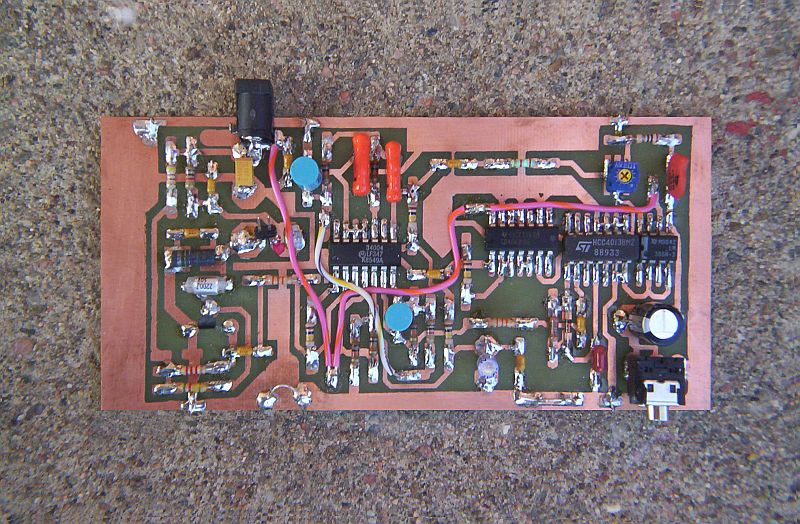
Detector/Demodulator Board Jumper List
| The demodulator board requires 4 wire jumpers. These are added to the top of the board. Use insulated wire. |
| Connect | to |
| A (V+) | A (U1 pin 4) |
| A (U1 pin 4) | A (U2 pin 14) |
| A (U2 pin 14) | A (U4 pin 6) |
| B (R13) | B (R12) |
Combined Modulator/Demodulator Parts List(Shopping List)Quantity - Value or part number 1 - 220pF (mica or metallized film) 2 - cases (if used) (user selected) Closing notes:
Here's what it's supposed to look like:![]() PCB layouts by John West, KB0ONB. |